- 您现在的位置:买卖IC网 > Sheet目录338 > LTC3230EUD#PBF (Linear Technology)IC LED DRIVR WHITE BCKLGT 20-QFN
�� �
�
�LTC3230�
�APPLICATIONS� INFORMATION�
�V� IN� and� CPO� Capacitor� Selection�
�The� style� and� value� of� the� capacitors� used� with� the� LTC3230�
�determine� several� important� parameters� such� as� regulator�
�control� loop� stability,� output� ripple,� charge� pump� strength�
�and� minimum� start-up� time.�
�To� reduce� noise� and� ripple,� it� is� recommended� that� low�
�equivalent� series� resistance� (ESR)� ceramic� capacitors�
�are� used� on� both� V� IN� and� CPO.� Tantalum� and� aluminum�
�capacitors� are� not� recommended� due� to� high� ESR.�
�The� value� of� C� CPO� directly� controls� the� amount� of� output�
�ripple� for� a� given� load� current.� Increasing� the� size� of� C� CPO�
�will� reduce� the� output� ripple� but� will� increase� start-up�
�time.� The� peak-to-peak� output� ripple� of� the� 1.5x� mode� is�
�approximately� given� by� the� expression:�
�times.� Since� the� nonoverlapping� time� is� small� (~10ns),�
�these� missing� “notches”� will� result� in� only� a� small� pertur-�
�bation� on� the� input� power� supply� line.� Note� that� a� higher�
�ESR� capacitor� such� as� tantalum� will� cause� a� higher� input�
�noise� due� to� the� higher� ESR.� Input� noise� can� be� further�
�reduced� by� powering� the� LTC3230� through� a� very� small�
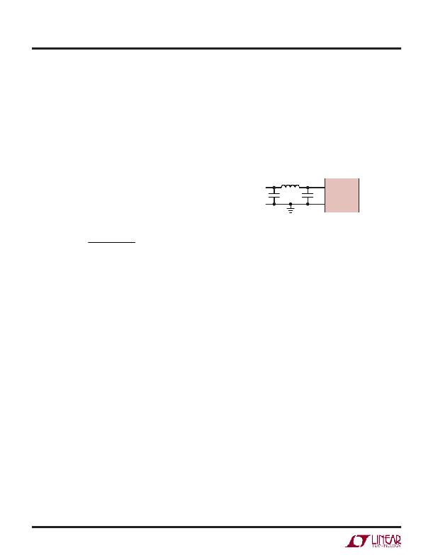
�series� inductor� as� shown� in� Figure� 5.� A� 10nH� inductor� will�
�reject� the� fast� current� notches,� thereby� presenting� a� nearly�
�constant� current� load� to� the� input� power� supply.�
�V� BAT�
�LTC3230�
�GND�
�3230� F05�
�3� ?� f� OSC� CPO�
�V� RIPPLE� (� P� -P)� =�
�I� OUT�
�?� C�
�Figure 5. 10nH Inductor Used for Input Noise Reduction�
�Flying� Capacitor� Selection�
�where� f� OSC� is� the� oscillator� frequency,� typically� 900kHz,�
�and� C� CPO� is� the� output� storage� capacitor.�
�The� output� ripple� in� 2x� mode� is� very� small� due� to� the� fact�
�that� load� current� is� supplied� on� both� cycles� of� the� clock.�
�Both� style� and� value� of� the� output� capacitor� can� signi?-�
�cantly� affect� the� stability� of� the� LTC3230.� As� shown� in� the�
�Block� Diagram,� the� LTC3230� uses� a� control� loop� to� adjust�
�the� strength� of� the� charge� pump� to� match� the� required�
�output� current.� The� error� signal� for� the� loop� is� stored�
�directly� on� the� output� capacitor.� The� output� capacitor�
�also� serves� as� the� dominant� pole� for� the� control� loop.� To�
�prevent� ringing� or� instability,� it� is� important� for� the� output�
�capacitor� to� maintain� at� least� 0.6μF� of� capacitance� over�
�all� conditions.�
�In� addition,� excessive� output� capacitor� ESR� >100m� Ω� will�
�tend� to� degrade� the� loop� stability.� Multilayer� ceramic� chip�
�capacitors� typically� have� exceptional� ESR� performance� and�
�when� combined� with� a� tight� board� layout� will� result� in� very�
�good� stability.� As� the� value� of� C� CPO� controls� the� amount�
�of� output� ripple,� the� value� of� C� VIN� controls� the� amount� of�
�ripple� present� at� the� input� pin� (V� IN� ).� The� LTC3230’s� input�
�current� will� be� relatively� constant� while� the� charge� pump�
�is� either� in� the� input� charging� phase� or� the� output� charging�
�phase� but� will� drop� to� zero� during� the� clock� overlapping�
�Warning:� Polarized� capacitors� such� as� tantalum� or�
�aluminum� should� never� be� used� for� the� ?ying� capaci-�
�tors� since� their� voltage� can� reverse� upon� start-up� of� the�
�LTC3230.� Ceramic� capacitors� should� always� be� used� for�
�the� ?ying� capacitors.�
�The� ?ying� capacitors� control� the� strength� of� the� charge�
�pump.� In� order� to� achieve� the� rated� output� current� it� is�
�necessary� to� have� at� least� 0.6μF� of� capacitance� for� each�
�of� the� ?ying� capacitors.� Capacitors� of� different� materials�
�lose� their� capacitance� with� higher� temperature� and� voltage�
�at� different� rates.� For� example,� a� ceramic� capacitor� made�
�of� X7R� material� will� retain� most� of� its� capacitance� from�
�–40°C� to� 85°C,� whereas� a� Z5U� or� Y5V� style� capacitor� will�
�lose� considerable� capacitance� over� that� range.� Capacitors�
�may� also� have� a� very� poor� voltage� coef?cient� causing� them�
�to� lose� 60%� or� more� of� their� capacitance� when� the� rated�
�voltage� is� applied.� Therefore,� when� comparing� different�
�capacitors,� it� is� often� more� appropriate� to� compare� the�
�amount� of� achievable� capacitance� for� a� given� case� size�
�rather� than� comparing� the� speci?ed� capacitance� value.� For�
�example,� over� rated� voltage� and� temperature� conditions,�
�a� 1μF,� 10V,� Y5V� ceramic� capacitor� in� a� 0603� case� may� not�
�provide� any� more� capacitance� than� a� 0.22μF,� 10V,� X7R�
�available� in� the� same� case.� The� capacitor� manufacturer’s�
�data� sheet� should� be� consulted� to� determine� what� value�
�3230fa�
�12�
�发布紧急采购,3分钟左右您将得到回复。
相关PDF资料
LTC3452EUF#TRPBF
IC LED DRIVER PHOTO FLASH 20-QFN
LTC3453EUF#TRPBF
IC LED DRIVER PHOTO FLASH 16-QFN
LTC3454EDD#TRPBF
IC LED DRIVER PHOTO FLASH 10-DFN
LTC3490EDD#PBF
IC LED DRIVER PHOTO FLASH 8-DFN
LTC3783EFE#PBF
IC LED DRVR PWM CONTROL 16-TSSOP
LV5026MC-AH
IC LED DRIVER 1CH HV 10SOIC
LV5213LP-TE-L-E
IC LED DVR 3CH CELL PHONE VCT16
LV5216CS-TE-L-E
IC LED DRIVER 10CH CELL 36WLP
相关代理商/技术参数
LTC3230EUD#TRPBF
功能描述:IC LED DRIVR WHITE BCKLGT 20-QFN RoHS:是 类别:集成电路 (IC) >> PMIC - LED 驱动器 系列:- 标准包装:6,000 系列:- 恒定电流:- 恒定电压:- 拓扑:开路漏极,PWM 输出数:4 内部驱动器:是 类型 - 主要:LED 闪烁器 类型 - 次要:- 频率:400kHz 电源电压:2.3 V ~ 5.5 V 输出电压:- 安装类型:表面贴装 封装/外壳:8-VFDFN 裸露焊盘 供应商设备封装:8-HVSON 包装:带卷 (TR) 工作温度:-40°C ~ 85°C 其它名称:935286881118PCA9553TK/02-TPCA9553TK/02-T-ND
LTC3230EUD-PBF
制造商:LINER 制造商全称:Linear Technology 功能描述:5-LED Main/Sub Display Driver with Dual LDO
LTC3230EUD-TRPBF
制造商:LINER 制造商全称:Linear Technology 功能描述:5-LED Main/Sub Display Driver with Dual LDO
LTC3240
制造商:LINER 制造商全称:Linear Technology 功能描述:3.3V/2.5V Step-Up/ Step-Down Charge Pump DC/DC Converter
LTC3240-2.5
制造商:LINER 制造商全称:Linear Technology 功能描述:Wide VIN Range, Low Noise, 250mA Buck-Boost Charge Pump
LTC3240-3.3
制造商:LINER 制造商全称:Linear Technology 功能描述:Wide VIN Range, Low Noise, 250mA Buck-Boost Charge Pump
LTC3240EDC-2.5
制造商:LINER 制造商全称:Linear Technology 功能描述:3.3V/2.5V Step-Up/ Step-Down Charge Pump DC/DC Converter
LTC3240EDC-2.5#TRMPBF
功能描述:IC REG MULTI CONFIG 2.5V 6DFN RoHS:是 类别:集成电路 (IC) >> PMIC - 稳压器 - DC DC 开关稳压器 系列:- 产品培训模块:Lead (SnPb) Finish for COTS
Obsolescence Mitigation Program 标准包装:50 系列:- 类型:升压(升压) 输出类型:两者兼有 输出数:1 输出电压:5V,2 V ~ 16.5 V 输入电压:2 V ~ 16.5 V PWM 型:- 频率 - 开关:45kHz 电流 - 输出:50mA 同步整流器:无 工作温度:0°C ~ 70°C 安装类型:通孔 封装/外壳:8-DIP(0.300",7.62mm) 包装:管件 供应商设备封装:8-PDIP